Optoelectronics devices on gallium nitride
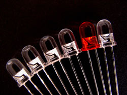
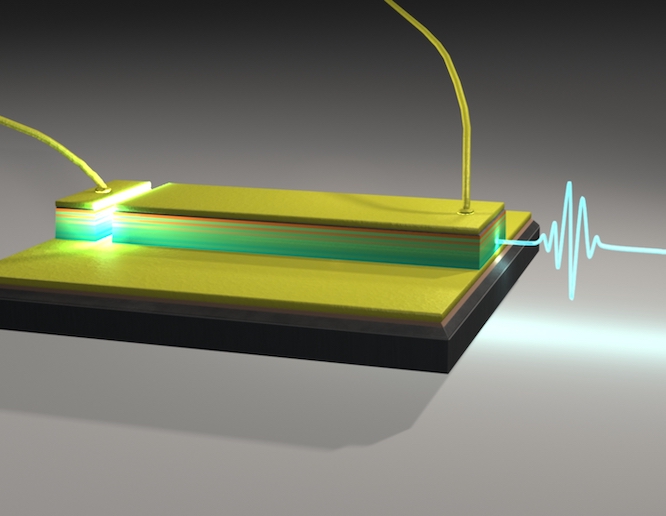
Gallium nitride (GaN) and its related alloys have opened up the road to efficient solid state lighting with white light emitting diodes (LEDs) replacing conventional fluorescent tubes. GaN-based high-frequency electronic devices for wireless applications have already been launched on the open market. Currently, they are beginning to revolutionise the field of high capacity data storage with blue laser diodes. Nevertheless, the hetero-epitaxial growth on foreign substrates, such as sapphire or silicon carbide (SiC), results in high defect density, limiting the luminous efficacy of GaN-based devices. On account of the recognised potential of GaN-based devices, the DENIS project, funded through the Fifth Framework Programme, aimed to develop a technique suitable for large-scale production of GaN thin wafers. The use of substrates with closely matching thermal expansion coefficients and lattice constants would provide the optimal solution to improving the performance and lifetime of GaN-based devices. The DENIS project has come to an end, having produced a range of positive contributions to the establishment of GaN technology in Europe. A technique and a reactor suitable for the growth of GaN boules from which thin wafers can be produced has been developed at the Linkoeping University in Sweden. More specifically, the Hydride-Vapour-Phase Deposition technique was successfully used for the growth of up to 2 inches in diameter GaN substrates with a thickness of 2mm. Growth of bulk GaN material was performed in a vertical hot-walled reactor at atmospheric pressure. When combined with the laser-induced lift-off for substrate delamination, the anticipated improved performance of light-emitting devices compared to the use of sapphire substrates was demonstrated. However, critical questions remain to be solved as well as the need to clarify the effect that the use of such substrates has on devices properties.


