Miniscule structures promise big efficiencies
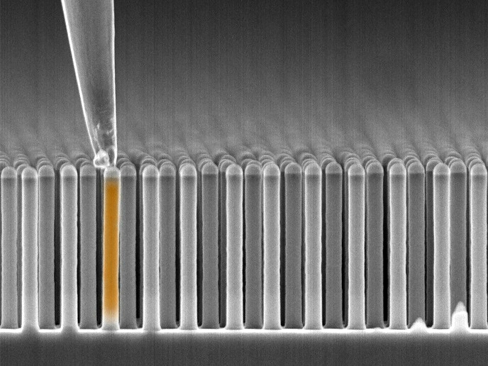
Silicon (Si), the current photovoltaic industry standard, is limited in the wavelength range it can 'see' and absorb. However, when strained Si is irradiated with light ions, miniscule voided structures are formed. These nanodots and nanovoids exhibit electronic and optical properties that had not been hitherto investigated in photovoltaic applications. Researchers initiated the NOVOSIP (Nano-voids in strained silicon for plasmonics) project to explore the use of nanodots and nanovoids to enhance the efficiency of single-crystalline Si photovoltaics. To this end, they created such plasmonic structures in a unique photovoltaic device configuration made of Si-tin (Sn) and Si layers put together. Nanodots and nanovoids were placed in the highly doped emitter layer close to the p-n junction in order to extend near-field effects. These effects were expected to contribute to carrier multiplication and increase light scattering, both promising to enhance sunlight absorption. Researchers then used different methods to investigate the structural, optical and electronic properties of each layer. Through high-temperature ion irradiation of the Si/SiSn/Si structure, the NOVOSIP team obtained spherical nanovoids in nanometre-sized strained Sn precipitates. With carbon ion implantation and subsequent thermal treatment, they observed carbon nanoflakes being formed. The flakes' crystalline structure allowed the absorption of all light wavelengths, potentially increasing the energy conversion rate. An innovative concept was also proposed and demonstrated for the self-assembly of metallic nanoshells in the strained Si/SiSn/Si structure. The results of theoretical investigations and numerical simulations reproducing different effects of plasmonic resonance helped the researchers to distinguish their contribution to the experimental observations. NOVOSIP work, although at an early stage, represents a promising path forward for single-crystalline Si solar cell research. The miniscule plasmonic structures engineered in strained Si multilayers enable enhanced light harvesting at low cost. Moreover, potential applications are already foreseen in gas-sensing and light-emitting devices.
Keywords
Photovoltaic cells, silicon, nanodots, nanovoids, NOVOSIP, plasmonics, energy conversion


