Silicon solar cells get a charge from nanowire top layers
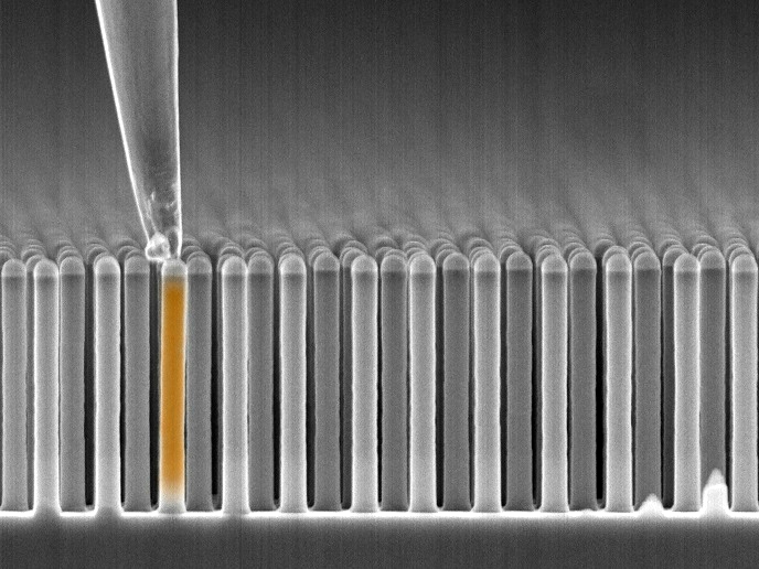
Silicon continues to dominate the solar cell industry. However, emerging technologies are using it in innovative ways. Exploiting tried and tested silicon as a base cell in tandem with nanowires of III-V semiconductors (alloys of elements from Group III and Group V of the Periodic Table) as the top cell, the EU-funded Nano-Tandem project set out to break barriers to increasing efficiency at lower cost. Breakthroughs in nanowire function and cost Nanowires are very tiny rods, approximately 100 nanometres wide and 10 micrometres long. The tandem cell exploits them in vertical configuration with about 6-7 million nanowires per square millimetre of cell. Template-assisted selective epitaxy (TASE) was used for growth of nanowires directly on silicon. Using this process, researchers demonstrated active p-n junctions in indium gallium phosphide (InGaP) nanowires grown with TASE. Nanowire nucleation on a III-V substrate rather than on silicon provided more than seven-fold improvement in the efficiency of indium phosphide (InP) nanowire solar cells – a record 15 %. Functional nanowires require tunnel diodes, something that has been quite challenging to achieve. Nano-Tandem removed this roadblock, demonstrating the ability to produce InP/InGaP nanowire tunnel diodes for the first time. Characterisation of the tunnel diodes by electron-beam-induced current (EBIC) was integral to improving alloy composition and thus the quality of the diodes. To transfer the nanowires to silicon, scientists embedded them in a polymer membrane, peeled the membrane off, and bound it to its new bottom cell. After three uses, the original substrates were unchanged, supporting even more uses and further cost savings. Finally, the team optimised a highly promising technique, aerotaxy, that enables growth of nanowires from seed particles directly in the gas phase without a substrate. Growth rates are 100–1 000 times faster than in conventional epitaxial growth, promising a radical reduction in cost. Project coordinator Lars Samuelson explains: “Forming the aerotaxy nanowires into a membrane was really challenging.” Nano-Tandem scientists benefited from a specialised ink process for aligning the wires. With this high-throughput technique, the team fabricated high-quality gallium arsenide (GaAs) nanowire p-n junctions. According to project leaders: “The expected price of a 28 % efficient GaAs/Si nanowire tandem module produced with the aerotaxy process is 0.296 USD/W. The expected future price of conventional crystalline silicon modules is 0.39 USD/W for a 25 % efficient module.” Higher efficiency at a significantly lower cost should make Nano-Tandem’s solar-cell technology a winner for global renewable energy markets. Innovative light-trapping for nanowire-based solar cells Conventional high-efficiency silicon solar cells use light-trapping mechanisms that exploit front-side structuring to boost absorption. This is not an option for tandem nanowire/silicon solar cells, so Nano-Tandem developed a rear-side photonic-light-trapping structure. With it, scientists achieved a new world record in conversion efficiency (33.3 %) for a tandem III-V/silicon thin-film solar cell. Applications in solar energy and beyond Nano-Tandem’s process optimisation and characterisation developments have improved nanowire growth and functionality, while enhancing the efficiency of the silicon-bottom cell. Detailed results can be found in the 38 peer-reviewed scientific publications. Outcomes pave the way to low-cost large-area tandem-nanowire III-V/silicon solar cells and European leadership in the growing PV market. They should also generate innovation in devices including LEDs, microelectronics and sensors.
Keywords
Nano-Tandem, nanowire, silicon, solar cell, tandem, efficiency, III-V, aerotaxy, tunnel diode, low-cost, TASE


