Fast and precise microsystem manufacturing
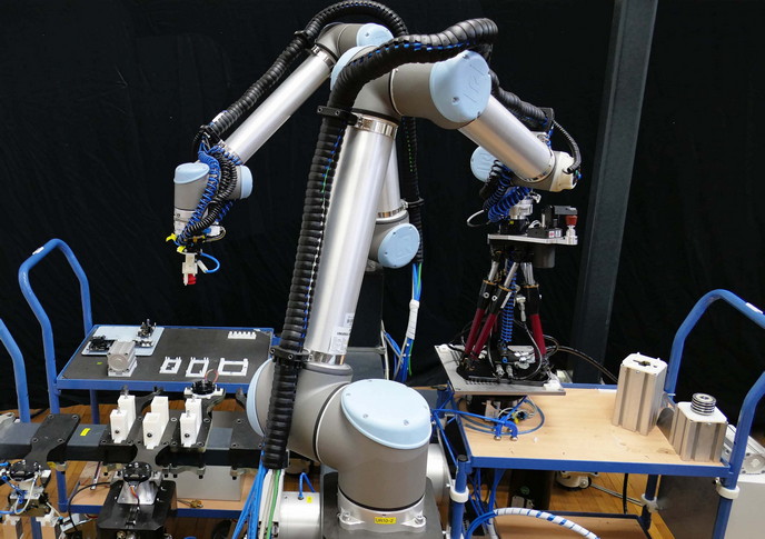
Forecasts regarding the evolution of the semiconductor industry and integrated circuit (IC) fabrication suggest that shrinking component dimensions will not be sufficient to achieve performance and cost benefits in smaller volumes. Three-dimensional (3D) integration is an emerging technology that may provide the solution to the density problem. It can be used to form vertically stacked and connected materials and components with a number of important benefits. Among these are reduced power, packaging and costs with increased performance. European researchers initiated the ‘Efficient and precise 3D integration of heterogeneous microsystems from fabrication to assembly’ (FAB2ASM) project to develop technology for high-throughput and precise 3D integration for microelectronics. Current integration technology for 3D microsystems relies on robotic machines and machine vision which must sacrifice speed for precision and vice versa. The FAB2ASM consortium is developing hybrid assembly technology combining robotic tools with self-alignment processes based on physical forces acting at the micro-scale. The consortium has already developed the necessary components, tools, and self-assembly and joining technologies as well as the joining materials. It has also designed three different industrial demonstrators. Tests on industry samples demonstrate ability to handle small and thin microchips, ultra-high chip-assembly speed and very high precision. FAB2ASM should have no problems reaching its goal of simultaneously fast and accurate 3D integration technology for multifunctional microsystems, overcoming the current bottleneck to commercialisation. Exploitation of the technology will no doubt have important impact on European nano- and micro-manufacturing, enabling competitive production of innovative products that would otherwise have to be outsourced.


