Carbon nanotubes from lab to market
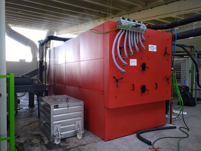
The carbon in CNTs is in the form of graphite – it was first observed serendipitously in pencil lead. When magnified, CNTs resemble rolled up chicken wire, albeit on the order of the size of atoms and molecules. CNTs have amazing mechanical strength as well as interesting electrical properties, acting as either metals or semiconductors depending on geometrical variations. They have captured the imagination of many for their potential use in a huge variety of novel applications. However, the most common production process, laser ablation, is quite expensive and not easily scaled up to industrial manufacturing capacity. European researchers sought to develop inexpensive channel spark ablation (CSA) technology to produce high quality single-walled CNTs (SWCNTs) by the tonne through funding of the Nanospark project. Scientists first developed the necessary CSA-based machinery for SWCNT production. Energy consumption of CSA manufacturing is typically on the order of 100 times less than conventional laser ablation creating the possibility of a tremendous decrease in production cost and final product price. In addition, installation costs are often up to five times cheaper. CNTs were produced using the new Nanospark equipment with potential commercialisation as powders, suspensions and dispersions in thin films (among the prominent media in high demand). Nanospark’s demonstrated production of large quantities of high quality CNTs with significant cost savings should have important impact on moving numerous CNT-based concepts from lab to market. Immediate goals are application to solar cells where a potential 50 % cost savings is expected compared to conventional crystalline cell modules.


