Novel semiconductor materials
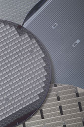
Silicon carbide is dark to light green in colour and has the chemical formula SiC. It is usually produced in an electric arc furnace and has been extensively used as an abrasive and structural material. It is also however a wide band-gap semiconductor currently under active development for high power, temperature, and frequency device applications. The interest in this material stems from its high electron mobility in relation to a phenomenon called polytypism. SiC crystals exhibit many structures depending on the stacking sequence of Si-C tetrahedra. The main SiC polytypes that have been explored have either the cubic (3C) or the hexagonal (4H or 6H) structures. It is the 3C structure that has the highest electron mobility, the smaller band-gap and it is therefore exceptionally suited for medium power applications (300-1200V, 10-100A). However, interest has concentrated on the hexagonal polytypes because of the commercial availability of substrates cut from bulk crystals. The SOLSIC project has rectified this problem by developing bulk cubic SiC crystals and wafers while at the same time cubic SiC properties were scrutinised. Several types of rectifiers like Schottky barrier diodes and various types of transistors like metal-oxide-semiconductor field-effect transistors (MOSFET) were developed based on 3C-SiC. A processing line for the fabrication of these devices has been established. Processing includes epitaxial growth of n- and p-doped layers, ion implantation and post-implantation annealing, lithography, dry etching, silicon dioxide and silicon nitride deposition, and thermal oxidation. The devices thus fabricated match in performance the corresponding state of the art hexagonal SiC devices. Crystal defects that initially inhibited performance from reaching the expected values were greatly reduced. In conclusion, it was demonstrated that for medium power applications, 300 to 600 Volts, devices fabricated from cubic silicon carbide perform exceptionally well.


