Rethinking silicon wafer technology
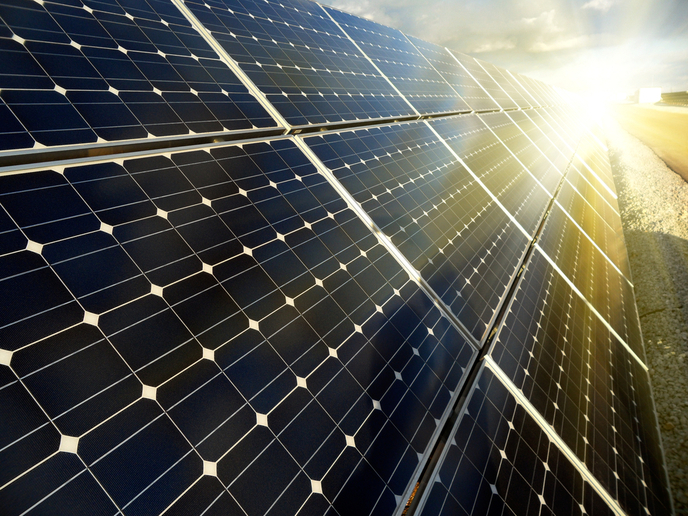
The photovoltaic (PV) industry in Europe has been growing rapidly, so much so that the necessary raw materials are in short supply. This is not only slowing PV adoption but driving up the price of the technology. The Energy, Environment and Sustainable Development Programme funded the TREASURE project to reverse this worrisome trend by investigating alternative sources of silicon. Physicists with the University of Konstanz in Germany contributed their experience in PV manufacturing to the TREASURE consortium. During the project they developed a reactor to create wafers from metallurgical silicon using Liquid Phase Epitaxy (LPE), which enables extremely thin but uniform silicon deposition. After successful laboratory trials, the German physicists assessed the potential benefits of expanding to industrial scale production. By combining several reactors in parallel, they estimated that enough wafers could be produced in one year to provide six megawatts of power. The cost per wafer is less than 10 cents and energy payback periods are very attractive, in the order of just a few days. Further to these encouraging results, the University of Konstanz is seeking patent protection for its new reactor. Driving down the cost per Watt (€/Wp) will provide impetus to the PV market and assist Europe in meeting the challenging goals set for electricity production from solar power.


