EU backs 3D laser printer project for the masses
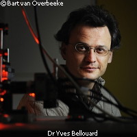
A European team of researchers is kick starting an EU-funded project with the aim of providing users with the tools they need to produce their own microsystems with nanoscale features for a lot less money and without big enterprise help. FEMTOPRINT ('Femtosecond laser printer for glass microsystems with nanoscale features') has clinched almost EUR 2.5 million in EU support to develop a 3D (three dimensional) printer for these microsystems, which are made of glass and are destined for use in research, academia and industry. The FEMTOPRINT project is backed by the 'Nanosciences, nanotechnologies, materials and new production technologies' Theme of the Seventh Framework Programme (FP7). Coordinated by the Eindhoven University of Technology (TUE) in the Netherlands, the FEMTOPRINT partners say their 'femtoprinter' is the answer users need to form 3D patterns in glass material by using a low-power femtosecond (1 quadrillionth of a second) laser beam. Despite their super mini size, microsystems are unique in that they can help power up various devices. Mechanical and electric components are commonly found inside microsystems that help these tiny machines measure signals and drive components. For instance, accelerometers (electromechanical devices that measure acceleration forces) are used in the computing world for their capacity to protect hard drives in laptops. If you drop your laptop, you can breathe a sigh of relief knowing that the accelerator detects the sudden fall and switches off the hard drive so that the damage is contained. The problem, however, is the high cost of producing microsystems. But their high price is just one headache; these mini machines also consume a lot of energy and need to be manufactured in a special 'cleanroom'. FEMTOPRINT project leader Dr Yves Bellouard of TUE's Department of Mechanical Engineering contends that the sluggish development of these microsystems can be attributed these problems. He explained that only large enterprises have the resources needed to get these microsystems out of the laboratory and into the real world. Dr Bellouard also notes that an investment is considered lucrative only when the market actually needs substantial amounts of these microsystems. So the biggest losers are the tiny, innovative companies and applications that are too specialised to go up against the big guns. And this is where FEMTOPRINT enters the picture: the partners use the femtosecond laser to create 3D patterns in glass. The properties of the glass change in the areas that are exposed to the laser light, depending on the intensity of that light, according to the researchers. So users can adjust the refractive index of the material, which the team says is a significant optical characteristic. The outcome is that the selected pattern is converted into a type of road network for the conduction of light. Optical motion sensors and optical computer chips could also benefit from this innovative development. The FEMTOPRINT partners point out that the laser light can have an impact on the chemical properties of the glass. The applied 3D pattern can be etched in one step compared to traditional methods that require patterns to be developed layer by layer. The upshot of this process is that because the pattern is applied in the interior of the glass, there is no contact with the air and no cleanroom is needed. The project partners hope to reduce this femtosecond laser for glass micro and nano manufacturing to a shoe-boxed size by 2015. FEMTOPRINT, which brings together French, German, Dutch, Swiss and UK experts, also seeks to bring the femtoprint laser to market with the creation of a consortium spin-off. Diverse industrial sectors will profit from such a development, and there is great potential for economic gains as well.
Countries
Switzerland, Germany, France, Netherlands, United Kingdom


