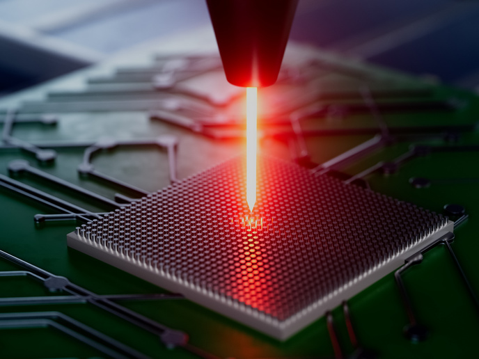
A low-noise, high-performance, coin-sized femtosecond laser
From studying materials and molecules to optical telecommunications, quantum technology and optical spectroscopy, femtosecond lasers have the potential to redefine research and innovation. The challenge is that these lasers – which use optical resonators to generate ultrashort, high-power pulses – are both large and expensive. But that is starting to change, thanks in part to the work of the EU-funded FEMTOCHIP project. The project aimed to provide femtosecond laser functionality but via a much smaller and less expensive package. Namely, a microchip. “By bringing together experts in ultrafast laser technology, micro-integration, materials science, and industrial applications, our goal was to overcome the many technical hurdles that have so far made femto-custom lasers on chips impossible,” says Franz Kärtner, group leader at the German Electron Synchrotron DESY, the project’s coordinating partner.
A more powerful laser from a compact, silicon photonics platform
What the project delivered was a thick-waveguide silicon-based integration platform for photonic integrated circuits that can be used to create complex circuitry based on silicon nitride. The high-power-integrated and mode-locked laser offers a peak power that reaches beyond 100 watts (W) and a pulse width of sub-100-femtoseconds for low timing jitter pulse generation applications. The project also demonstrated very high-power optical amplifiers capable of increasing the output power level close to 2 W. “Prior to our work, the maximum output power from an integrated device was a mere 2 milliwatts from a semiconductor amplifier,” explains Neetesh Singh, a senior scientist at DESY. “If we compare our solution to the best integrated amplifiers from the past 30 years, regardless of wavelength, then our results are 10 times higher.” Other key results include the first very high-energy Q-switched integrated laser, a wideband apodised grating reflector, and a chirped pulse amplifier demonstrating 800 W peak power at the output. The project also demonstrated a pulse interleaver that increases the repetition rate from 217 megahertz to 14 gigahertz – all from a compact, silicon photonics platform. “Not only are our results comparable to many fibre-based systems, they clearly outperform even the best standalone semiconductor optical amplifiers and offer pristine beam quality,” adds Singh.
Addressing real-world challenges using silicon photonics
The FEMTOCHIP project has laid the foundation for low-noise, high-performance, coin-sized femtosecond laser technology that will be available to science and industry at a fraction of the usual cost. These lasers could serve as an exceptionally powerful platform for a multitude of applications. For example, the FEMTOCHIP solutions could act as a seed laser used to build up complex high-power femtosecond laser sources. Thanks to its extremely low jitter, it could also act as a clock and sampler for photonic-based analogue-to-digital converters, taking timing and positioning systems to the next level. “Achieving an unprecedented level of output power now allows silicon photonics to be explored in the sense of high power from a miniature system, which makes silicon photonics truly applicable to real-world challenges,” concludes Kärtner.
Keywords
FEMTOCHIP, femtosecond laser, microchip, laser, materials science, silicon photonics, circuits