Single-crystal organic devices with logic operations closer to reality
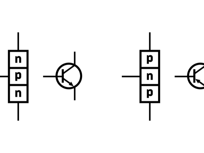
Organic electronics have the potential to revolutionise technology with their high cost efficiency, versatility and light weight compared with conventional electronics. Made of widely available and less toxic materials, organic electronics are ideal for applications that require flexibility and adaptability to large areas. Organic materials can be used as conductive inks for printing electronic circuits at a low cost. Organic light-emitting diodes, organic field-effect transistors (OFETs) and organic photovoltaics are the biggest success stories of the field so far. Charge transport is an important concept to describe the operation principles and performance of organic semiconductors. Depending on whether the majority of charge carriers in the crystal are positive holes or negative electrons, semiconductors are classified into p and n types, respectively. Use of both p- and n-type semiconductors proves a boon to complementary logic devices embedded in electronic circuits. The PARADA project successfully demonstrated growth of parallel single-crystal stripes of p- and n-type semiconductors in an effort to fabricate single-crystal transistors that can perform logic operations. Electronic devices comprising single-crystal transistors display highly desirable properties: high charge-carrier mobility, low defect concentration and high operational stability. Funded by the Marie Skłodowska-Curie programme, the project demonstrated innovations on several fronts.
Crystal growth of semiconductor mixtures
Growing organic semiconductors as single crystals that can transport either electrons or holes is not new. For example, the OFET fabrication process requires the separate deposition and patterning of two different semiconducting materials, one for each transistor type. The process requires selection of the most suitable semiconductors in terms of size and shape. Furthermore, the n- and p-type semiconductors need to display comparable electronic properties. Overall, the process is tedious and resembles craftwork. Semiconductors exhibiting ambipolar charge transport could greatly help address these challenges. The concept involves injecting and transporting electrons and holes in a single semiconducting layer. PARADA focused on processing p- and n-type semiconductors using an efficient, solvent-free thin-film fabrication method. “Although there has been a flurry of research activities around the directional crystallisation of thin-film organic semiconductors growing from a melt, the crystal growth of semiconductor mixtures has been completely overlooked. PARADA has successfully demonstrated that the directional crystal growth of semiconductor mixtures can be expanded into organic semiconductors,” notes Guangfeng Liu, the research fellow who has been coordinating PARADA. Control of the phase separation in the organic semiconductor donor-acceptor mixture and the temperature gradient had a pronounced impact on the crystal growth rate. Researchers thoroughly studied the melt and crystal states of organic semiconductors using calorimetry and X-ray crystallography to identify the best combination of p- and n-type semiconductors. In their effort to obtain parallel stripes of p- and n-type semiconductors on glass substrates, they faced an unexpected problem: crack formation in the single crystals. To solve this, they coated rigid glass substrates with a soft rubber dielectric layer.
Next generation of high-performance, flexible and printed electronics
The fabrication and characterisation of OFETs based on the prepared crystalline films could not be completed due to the COVID-19 pandemic. “PARADA results could bring fresh momentum to the field of organic semiconductors for use in devices that perform logic operations. OFETs enable the manufacturing of inexpensive and flexible electronic devices, such as flat panel displays, radio frequency identification cards and electronic skins. These devices urgently need the development of complementary logic circuits to consume less energy,” concludes Liu.
Keywords
PARADA, organic semiconductors, OFET, n-type semiconductors, logic operations, single crystal, organic electronics, organic field-effect transistor