Scientists design 3D thin-film silicon solar-cells with better efficiency potential
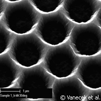
Thin-film solar cells without added silicon 'bulk' is the new creation of Czech and Swiss researchers and industry actors, who worked together to deliver a product that could deliver greater efficiency. The study was funded in part by the N2P ('Flexible production technologies and equipment based on atmospheric pressure plasma processing for 3D [three-dimensional] nano structured surfaces') project, which has clinched EUR 7.4 million under the 'Nanosciences, nanotechnologies, materials and new production technologies' (NMP) Theme of the EU's Seventh Framework Programme (FP7). The design is presented in the journal Applied Physics Letters. Researchers from the Academy of Sciences of the Czech Republic and experts from the Swiss-based group Oerlikon Solar Lab targeted the development of a long-term option for high-yield but low-cost industrial production of solar panels from raw materials. According to the team, these can be found in amorphous silicon solar cells and microcrystalline silicon tandem cells. The upshot is energy that is much more efficient. However, Milan Vanecek, who led the photovoltaic group at the Institute of Physics in Prague, pointed out a weakness of these cells: the stable panel efficiency is not nearly as high as the efficiency generated by crystalline wafer-based silicon, the item du jour. 'To make amorphous and microcrystalline silicon cells more stable, they're required to be very thin because of tight spacing between electrical contacts, and the resulting optical absorption isn't sufficient,' explains Dr Vanecek. 'They're basically planar devices. Amorphous silicon has a thickness of 200 to 300 nanometres, while microcrystalline silicon is thicker than 1 micrometre.' This sophisticated design, however, is centred on optically thick cells that are 'strongly absorbing', and the distance between the electrodes is steady. 'Our new 3D design of solar cells relies on the mature, robust absorber deposition technology of plasma-enhanced chemical vapour deposition, which is a technology already used for amorphous silicon-based electronics produced for liquid crystal displays,' the Czech researcher says. 'We just added a new nanostructured substrate for the deposition of the solar cell.' The researchers explain that the nanostructured substrate encompasses zinc oxide (ZnO) nanocolumns or a honeycomb array of microholes or nanoholes etched into the transparent conductive oxide layer. The team calls the latter design 'Swiss cheese'. 'This latter approach proved successful for solar cell deposition,' Dr Vanecek points out. 'The potential of these efficiencies is estimated within the range of present multicrystalline wafer solar cells, which dominate solar cell industrial production. And the significantly lower cost of Micromorph panels, with the same panel efficiency as multicrystalline silicon panels (12% to 16%), could boost its industrial-scale production.' The team said that they will continue their work to optimise and raise efficiency even further.For more information, please visit: Academy of Sciences of the Czech Republic:http://www.cas.cz/index.htmlOerlikon Solar Lab:http://www.oerlikon.com/solar/
Countries
Switzerland, Czechia


